
Printed Circuit Boards (PCBs) are the cornerstone of modern electronics, and the ASL106-05PN-HE component holds a significant role in various applications. This article dives deep into the ASL106-05PN-HE PCB footprint and symbol, explaining its importance, specifications, design strategies, and practical applications. Whether you’re an engineer, designer, or electronics enthusiast, this guide will empower you with insights to optimize its implementation.
What is ASL106-05PN-HE?
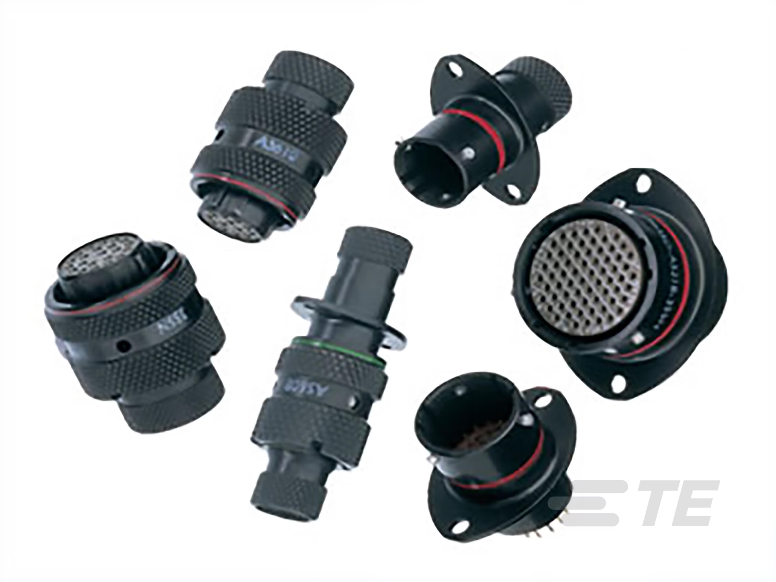
The ASL106-05PN-HE is a specialized electronic component commonly used in high-reliability circuits. Known for its robust design, it’s a connector type often found in aerospace, industrial, and consumer electronics. Understanding its PCB footprint and symbol is crucial for seamless integration into a PCB layout.
The footprint refers to the physical design layout of the component’s terminals on the PCB, ensuring proper alignment and electrical connection. The symbol, on the other hand, represents the component in schematic diagrams, providing essential details for circuit design and analysis.
Specifications of ASL106-05PN-HE
The ASL106-05PN-HE boasts distinct features that make it ideal for various demanding applications. Its key specifications include:
- Pin Count: 5 pins
- Mounting Type: Through-hole
- Material Composition: High-grade thermoplastic and metallic contacts for durability and conductivity
- Operating Voltage and Current: Suitable for applications demanding up to 250V and moderate current levels
- Temperature Range: Operates efficiently between -55°C and +125°C
The high precision and robust materials ensure long-term performance even in extreme conditions, making it a preferred choice for mission-critical systems.
Importance of the ASL106-05PN-HE PCB Footprint
The PCB footprint ensures the physical compatibility of the ASL106-05PN-HE with the printed circuit board. Proper footprint design prevents common issues like:
- Misalignment of solder pads
- Inconsistent solder joints
- Electrical connectivity failures
Designing the correct footprint involves considering dimensions, pin spacing, pad size, and thermal relief. Precise adherence to manufacturer guidelines minimizes rework and enhances reliability.
Understanding the ASL106-05PN-HE Symbol
The symbol of ASL106-05PN-HE simplifies circuit representation in schematic diagrams. It provides a clear visual reference to:
- Electrical connections
- Pin assignments
- Component functions
A well-drawn symbol aids in error-free PCB design, ensuring compatibility between schematic and layout stages.
Designing a PCB Footprint for ASL106-05PN-HE
Creating an accurate footprint involves following a systematic process:
- Collect Component Data: Refer to the manufacturer’s datasheet for dimensions and specifications.
- Define Pad Geometry: Calculate the size and spacing of the solder pads based on pin dimensions.
- Consider Solder Mask Clearance: Ensure proper spacing to avoid short circuits during soldering.
- Thermal Relief: Design thermal relief patterns for heat dissipation.
- Verification: Simulate and verify the design using PCB design software to confirm accuracy.
Key Challenges in Designing the ASL106-05PN-HE Footprint
Engineers face several challenges while designing the footprint, such as:
- Ensuring compliance with IPC standards
- Accommodating thermal management requirements
- Balancing mechanical strength with electrical performance
By addressing these challenges during the design phase, one can avoid costly errors during manufacturing.
Applications of ASL106-05PN-HE
The versatility of ASL106-05PN-HE enables its use in diverse fields, including:
- Aerospace Systems: Reliable performance under extreme conditions.
- Industrial Automation: Connectivity solutions for control circuits.
- Medical Equipment: Precision and durability for sensitive instruments.
- Consumer Electronics: Compact and efficient design for gadgets.
Its adaptability to various environments underscores its importance across industries.
Optimizing Circuit Performance with ASL106-05PN-HE
Integrating the ASL106-05PN-HE effectively into your design can enhance overall circuit performance. Here are some tips:
- Correct Placement: Position the component to minimize signal loss and interference.
- Adequate Clearance: Maintain spacing to prevent short circuits.
- Thermal Management: Employ proper heat dissipation techniques.
- Quality Soldering: Use high-quality soldering materials and techniques for robust connections.
Common Mistakes to Avoid with ASL106-05PN-HE
Avoiding mistakes during design and assembly is crucial. Common pitfalls include:
- Ignoring manufacturer specifications
- Poor solder pad design
- Inadequate thermal relief
- Misinterpreting schematic symbols
Attention to detail ensures smoother production and long-lasting performance.
Testing and Validation of the ASL106-05PN-HE
Testing ensures that the component functions as expected. Key testing procedures include:
- Electrical Tests: Verify voltage and current handling capabilities.
- Mechanical Stress Tests: Assess durability under mechanical loads.
- Thermal Analysis: Confirm performance across operating temperatures.
Proper validation boosts confidence in your design and reduces the risk of field failures.
Software Tools for Designing the ASL106-05PN-HE Footprint and Symbol
Various PCB design tools facilitate footprint and symbol creation. Popular options include:
- Eagle CAD: User-friendly interface for schematic and PCB layout design.
- KiCad: Open-source software with robust features for professionals.
- Altium Designer: Advanced features for high-precision PCB designs.
These tools streamline the design process, ensuring accuracy and efficiency.
Maintenance and Longevity of ASL106-05PN-HE
To ensure the longevity of circuits utilizing the ASL106-05PN-HE:
- Periodic Inspection: Check for signs of wear or corrosion.
- Preventive Maintenance: Replace worn-out components promptly.
- Environmental Protection: Shield components from moisture and contaminants.
These practices enhance reliability and extend the component’s life.
Environmental Impact of ASL106-05PN-HE
Understanding the environmental implications of electronics manufacturing is essential. The ASL106-05PN-HE complies with RoHS standards, ensuring minimal use of hazardous substances. Its recyclable materials also contribute to sustainability efforts.
FAQs
What are the key features of ASL106-05PN-HE?
ASL106-05PN-HE offers robust construction, high durability, and compatibility with through-hole mounting systems, making it ideal for demanding applications.
How do I design a PCB footprint for ASL106-05PN-HE?
Refer to the manufacturer’s datasheet, consider dimensions and spacing, and use PCB design software for precise layout creation.
What applications use ASL106-05PN-HE?
It is used in aerospace, industrial automation, medical equipment, and consumer electronics due to its reliability and versatility.
What software is best for designing the ASL106-05PN-HE symbol?
Popular options include Eagle CAD, KiCad, and Altium Designer, offering robust features for accurate designs.
Why is thermal management important for ASL106-05PN-HE?
Proper thermal management ensures efficient heat dissipation, preventing overheating and extending the component’s life.
Is ASL106-05PN-HE environmentally friendly?
Yes, it complies with RoHS standards and uses recyclable materials to reduce environmental impact.